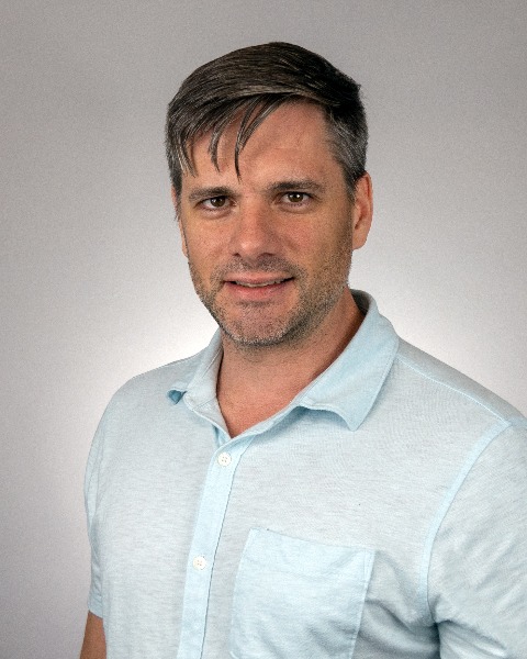
Edward Nelson
AFM Technical Specialist
Nanosurf / SPEC-TII
Woburn, MA, United States
Edward Nelson is a physicist and nanotechnology specialist with over 15 years of experience in atomic force microscopy (AFM) and surface characterization. At Nanosurf, he works closely with semiconductor and materials researchers to implement advanced AFM techniques for metrology applications, including roughness quantification, mechanical property mapping, and electrical characterization at the nanoscale.
Ed holds a Ph.D. in Physics from the University of Rochester, where his research focused on nanoscale interactions and nanoparticle-biological interfaces. His career spans roles in technical sales, applications development, and system integration, concentrating on translating cutting-edge AFM capabilities into reliable measurement workflows for process control and R&D. He has contributed to numerous scientific publications in AFM, nanopores, and scanning probe techniques.
Presentation(s):
-
High-Throughput Wafer Metrology: Roughness and Mechanical Mapping with Alphacen 300
Wednesday, October 8, 2025
3:10pm - 5:00pm MT
